Author: Godot
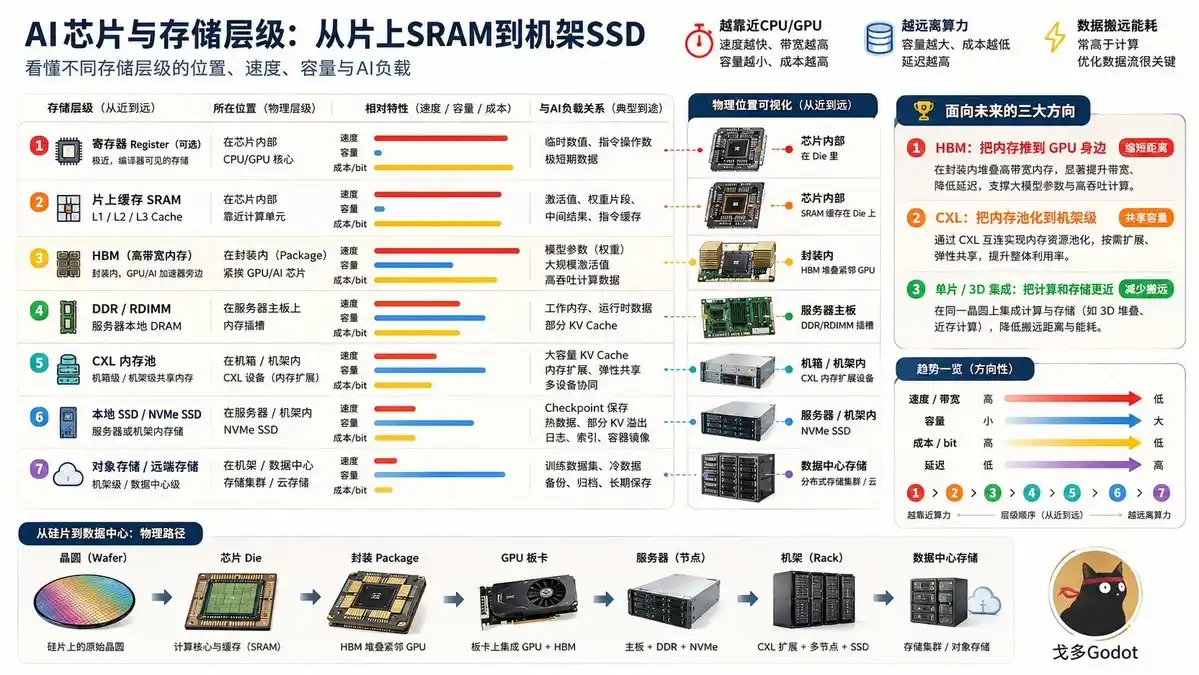
AI storage can be broken down into six layers,
1) On-chip SRAM
2) HBM
3) Motherboard DRAM
4) CXL Pooling Layer
5) Enterprise SSD
6) NAS and Cloud Object Storage
This hierarchy is based on the location of storage; the further down, the farther from the computing unit, and the larger the storage capacity.
In 2025, the total market for these six layers (SRAM is on compute chips, its embedded value needs to be excluded) was about $229 billion, with DRAM accounting for half, HBM for 15%, and SSD for 11%.
In terms of profit, each layer is highly concentrated among oligopolies, with the top three typically holding over 90% market share.
These profit pools can be divided into three categories,
1) High-margin oligopolistic pools at the silicon layer (HBM, embedded SRAM, QLC SSD)
2) High-margin emerging pools at the interconnect layer (CXL)
3) Scale-compounding pools at the service layer (NAS, Cloud Object Storage)
The three types of pools differ in nature, growth rate, and moats.
Why is Storage Layered?
Because the CPU responsible for control and the GPU responsible for computing only have temporary cache on the chip, namely on-chip SRAM cache. This cache space is too small, only enough to hold temporary parameters, and cannot accommodate large models.
Outside these two chips, larger external memory is needed to store the large models and the context for inference.
Computation is fast. The latency and energy consumption of moving data between different storage layers are the biggest issues.
Therefore, there are currently three main directions,
1) Stack HBM, placing memory next to the GPU to shorten the data transfer distance.
2) Use CXL to pool memory to the rack level, sharing capacity.
3) Integrate computing and storage on the same wafer, achieving compute-in-memory.
These three directions will shape the profit pool of each layer over the next five years.
The specific layers are detailed below,
L0 On-chip SRAM: A Profit Pool Exclusive to TSMC
SRAM (Static Random-access Memory) is the cache inside CPUs/GPUs, embedded in each chip and not traded separately.
The standalone SRAM chip market is only about $1–1.7 billion. Leaders are Infineon (~15%), Renesas (~13%), and ISSI (~10%)—a small market.
The profit pool for this part lies with TSMC. To fit more SRAM into each generation of AI chips, more wafers must be purchased.
Over 70% of the world's advanced process wafers are in TSMC's hands. The SRAM area of every H100, B200, TPU v5, etc., ultimately translates into TSMC's revenue.
L1 HBM: The Largest Profit Pool of the AI Era
HBM (High Bandwidth Memory) is high-bandwidth memory where DRAM (Dynamic Random-access Memory) dies are vertically stacked using TSV (Through-Silicon Via) technology and then attached next to the GPU via CoWoS packaging.
HBM almost single-handedly determines how large a model an AI accelerator can run. SK hynix, Micron, and Samsung have a near 100% market share.
As of Q1 2026, the latest market share breakdown is: SK hynix 57% to 62%, Samsung 22%, Micron 21%. SK hynix has secured significant procurement shares from companies like NVIDIA and is the dominant supplier.
Micron's Q1 FY2026 earnings call mentioned that the HBM TAM (Total Addressable Market) is expected to grow at a CAGR of ~40%, from about $35 billion in 2025 to $100 billion in 2028, reaching the $100 billion mark two years earlier than previous forecasts.
The core advantage of HBM lies in its extremely high profit margins. In Q1 2026, SK hynix's operating profit margin reached a record 72%.
Reasons for high profitability,
1) The TSV manufacturing process sacrifices some traditional DRAM capacity, keeping HBM in a state of supply shortage.
2) Improving advanced packaging yield is difficult; Samsung's previous market share drop from 40% to 22% was also affected by this.
3) Major suppliers have been relatively cautious in capacity expansion, and achieved a DRAM ASP (Average Selling Price) increase of over 60% QoQ in Q1 2026, demonstrating a clear seller's market.
Among the three giants, SK hynix, driven by strong HBM demand, achieved annual operating profit of 47.21 trillion KRW in 2025, surpassing Samsung Electronics for the first time in history. In Q1 2026, with a 72% operating margin, it even exceeded the profitability levels of TSMC (58.1%) and NVIDIA (65%).
Micron has high growth expectations, with Bank of America raising its target price to $950 in May 2026. Samsung, with the continuous progress of HBM4 mass production, has the largest room for market share recovery.
L2 Motherboard DRAM
This layer refers to what we commonly call memory modules (DIMMs).
Motherboard DRAM includes conventional memory products like DDR5, LPDDR, GDDR, MR-DIMM, etc. It is currently the part with the highest market sales share in the AI storage system. The global DRAM market reached approximately $121.83 billion in 2025.
Samsung, SK hynix, and Micron still dominate the vast majority of the market. According to the latest data from Q4 2025, Samsung ranked first with a 36.6% market share, SK hynix second with 32.9%, and Micron third with 22.9%.
The shift in production capacity towards higher-margin HBM has helped maintain high profitability and pricing power for memory. Although the single-product margin of conventional motherboard DRAM is not as high as HBM's, its overall market size is the largest.
L3 CXL Pooling Layer
CXL (Compute Express Link) allows DRAM to be "pooled" from a single server motherboard to the entire rack level.
With CXL 3.x and beyond, all memory in a rack can be shared and scheduled by multiple GPUs in the future, allocated on-demand. This solves the problem of KV cache, vector databases, and RAG indexes not fitting or being too cumbersome to move during AI inference.
The CXL memory module market was only $1.6 billion in 2024, projected to reach $23.7 billion by 2033. It appears the oligopoly of Samsung, SK hynix, and Micron will continue.
In this layer, Astera Labs focuses on Retimers and intelligent memory controllers between CXL and PCIe, holding about 55% share of this sub-market. Latest quarter revenue was $308 million, up 93% YoY; non-GAAP gross margin 76.4%; net profit up 85% YoY. It can be said to be quite lucrative.
L4 Enterprise SSD: The Biggest Beneficiary of the Inference Era
Enterprise NVMe SSDs are the main battleground for AI training checkpoints, RAG indexes, KV cache offloading, and model weight caching. High-capacity QLC SSDs have completely pushed HDDs out of AI data lakes.
The enterprise SSD market was about $26.1 billion in 2025, with a CAGR of 24%, projected to reach $76 billion by 2030.
As for the competitive landscape? Correct, still dominated by the three giants.
Market share by revenue in Q4 2025: Samsung 36.9%, SK hynix (including Solidigm) 32.9%, Micron 14.0%, Kioxia 11.7%, SanDisk 4.4%. The top five account for about 90%.
The biggest change in this layer is the explosion of QLC SSDs in AI inference scenarios. SK hynix's subsidiary Solidigm and Kioxia have already produced single-disk products with 122 TB capacity. AI inference KV cache and RAG indexes are spilling over from HBM to SSDs.
From a profit pool perspective, enterprise SSDs don't have the extreme gross margins of HBM but enjoy dual tailwinds of capacity-driven growth and inference expansion.
SK hynix (via Solidigm) and Kioxia are relatively pure plays. Samsung and SK hynix enjoy triple-layer benefits from HBM + DRAM + NAND, making them more comprehensive AI storage platform companies.
L5 NAS and Cloud Object Storage: The Compounding Pool of Data Gravity
NAS and Cloud Object Storage are the outermost layers for AI data lakes, training corpora, backup/archiving, and cross-team collaboration. In 2025, NAS was about $39.6 billion (CAGR 17%), and Cloud Object Storage about $9.1 billion (CAGR 16%).
Major vendors for enterprise file storage are NetApp, Dell, HPE, Huawei; for SMBs, Synology and QNAP. For Cloud Object Storage, using IaaS share estimates, AWS ~31–32%, Azure ~23–24%, Google Cloud ~11–12%, the three combined ~65–70%.
Profits in this layer mainly come from long-term hosting, data egress fees, and ecosystem lock-in.
To summarize,
1) DRAM has the largest market but the lowest gross margins (30–40%); HBM's market is only one-third of DRAM's, but its gross margin is double (60%+); CXL Retimers have the smallest market but the highest gross margin (76%+). The closer the layer is to computing, the scarcer and more lucrative it is.
2) Incremental profit pool growth primarily comes from three areas: HBM (CAGR 28%), Enterprise SSD (CAGR 24%), and CXL Pooling (CAGR 37%).
3) Each layer has different business barriers: HBM relies on technical barriers (TSV, CoWoS, yield ramp); CXL-type relies on IP and certification (single supply chain for Retimers); service-type relies on switching costs.